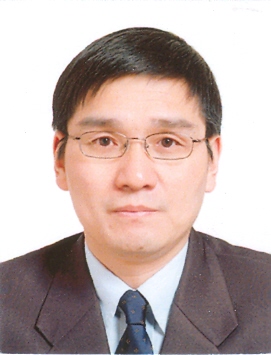
Professor Lianshan Wang, Institute of Semiconductors, Chinese Academy of Sciences
Email: ls-wang@semi.ac.cn
Telephone: 010-82304236/4314
Address: A35 Qinghua East road, Haidian, Beijing, china
Postcode: 100083
Research Areas
Wide-Bandgap Semiconductor Materials and Devices
Education
Feb. 1999, Ph. D (Semiconductor Materials), Institute of Semiconductors, Chinese Academy of Sciences, Beijing, China.
Aug. 1992, Master of Science (Condensed Matter Physics), Institute of Solid State Physics, Chinese Academy of Sciences, Hefei, Anhui Province, China.
June 1986, Bachelor of Science (Physics), Hubei University, Wuhan, Hubei Province, China
Experience
May 2013- , Professor at Key Laboratory of Semiconductor Materials Sciences, Institute of Semiconductors, Chinese Academy of Sciences
September 2009-April 2013, Professor at the Research Center for Semiconductor Lighting, Institute of Semiconductors, Chinese Academy of Sciences
October 2006-August 2009, Professor at Optoelectronic Device & Integration Division, Wuhan National Laboratory for Optoelectronics (WNLO), Huazhang Unversity of Science and Technology
February.2009-July 2009, Academic Visiting Professor at Department of Electrical and Electronic Engineering, University of Bath, in relation with NanoGaN Limited, UK
October 1999~ October 2006, Research Scientist at Opto- & Electronic Systems Cluster, Institute of Materials Research and Engineering, Singapore.
August 1998-July 1999, Visiting Scholar at Department of Electronic and Information Engineering of the Hong Kong Polytechnic University:
September 1992-August 1995, Assistant Researcher (a position equivalent to lecturer) at Center for Materials Research and Analysis, Wuhan University of Technology.
July 1986-August 1989, A teacher, Assistant Lecturer at Xinzhou Conunty’s Technical School.
Research Interests
Epitaxial growth and Processing of III-V Semiconductor Materials and devices
MOCVD epitaxial growth technology for III-nitride materials (e.g. bulk film, quantum well and quantum dot) and devices (blue/green/UV light-emitting diodes, blue/UV laser diodes, field effect transistors (FET), UV-detectors, solor cells).
Fabrication of light-emitting diodes (LEDs), semiconductor laser diodes (LDs), high electron mobility transistor (HEMT) , solar cells and detectors/arrays, including photolithography, wet/dry etching, deposition of dielectric films and metal electrodes, etc.
Materials and Device characterisation
Study on the physical properties of materials by photoluminescence (PL) and photoluminescence excitation (PLE), Raman scattering, high-resolution x-ray diffraction (XRD), Hall, CV DLTS, L-I, I-V, fT, fmax, Pout , PAP, measurements, etc.
Growth dynamics of MOCVD, HVPE and MBE
Reactor design, chemical reaction mechanism, hydrodynamics, fluid pattern simulation and boundary-layer theory.
Semiconductor Nanostructures for nano-optoelectronics
Research and develop (R&D) a capability in wide-bandgap semicondcutor nanostructures (nanowire, nanorod, naonobar, nanoring, etc.) for the future nanooptoelectronics on novel substrates.
Students
已指导学生
王建霞 博士研究生 080501-材料物理与化学
金东东 博士研究生 080903-微电子学与固体电子学
吉泽生 硕士研究生 085204-材料工程
李方政 博士研究生 080501-材料物理与化学
孟钰淋 博士研究生 080501-材料物理与化学
文玲 硕士研究生 085204-材料工程
柴若皓 硕士研究生 080501-材料物理与化学
现指导学生
李文龙 博士研究生 080501-材料物理与化学
Research Projects
NSFC Key instrument programme (Grant No. 51727901): “Time-space in-situ monitering and controlledly comprehensive instrument for film growth process”, 01/2018-12/2022, CNY 6345.5K
The National Key Research and Development Program of China (Grant No. 2017YFB0404203): The core equipement programme of third geration of semicondutor materials, No.3 Project “PVT and HVPE instruements toward for the large area AlN single crystal”, 07/2017-12/2020, CNY828K
NSFC Project (Grant No. 61774142): “Yellow-Orange Semipolar GaN-based Materials”, 01/2018-12/2021, CNY630K
Open Project of Si-based LED Engineering & Technologic Research Center Nanchuang University (Grant No. 2017001), “nonpolar/semipolar GaN materials on Si substrate”, 09/2017-08/2019, CNY1000K
